Passion fruit is a kind of fruit, which is mainly cultivated in tropical and subtropical regions. Fruit can be eaten raw or used as vegetables and feed. It has high economic value and is widely distributed in the warm and humid regions of southern China, especially in Hainan. In order to give full play to the advantages of regional characteristics of fruits, expand the planting area of ​​passion fruit and guarantee the planting efficiency, in the process of passion fruit planting, using soil moisture temperature instrument and other scientific instruments to carry out environmental testing is very necessary, soil moisture The monitoring data provided by the temperature meter can be the basis for passion fruit science cultivation and provide important technical support for it. 4 Layer PCB
4 Layer PCB
Four-layer circuit board is a kind of printed circuit board. It is made of four layers of glass fibre, which can reduce the cost of PCB.
There are also great differences between the 2-layer and 4-layer PCB. For details, please click: What's the difference between 2 layer and 4 layer PCBs?
4 layer PCB stackup include two inner layers, inner layer 1 and 2, are sandwiched between the top and bottom layers. From top to bottom, the 4-layer PCB stackup like below ,The top, i.e. the signal layer (0.0014 in. width) is followed by a prepreg layer with a thickness of 0.0091 in. and dielectric constant of 4.2. The top layer is copper material. The prepreg layer is followed by inner layer 1 (0.0014 in.), referred to as the plane. A core sublayer is part of inner layer 1, which has a width of 0.037 in. This is followed by inner layer 2, which is another plane layer made with 1 oz. copper and is 0.0014 in. thick. Another prepreg sublayer constituting two sheets that are 0.0091 in. thick forms part of inner layer 2. The final layer, the bottom layer, is also 0.0014 in. thick, and is a signal layer as well. Interconnects are soldered and placed on the top and bottom layers.
The standard 4-layer PCB stack is shown below, and GND and VCC can be switched according to the layer with more signals.
If you don't want to connect all the ground pins through the hole, there will be different stacks and wide power routing on the signal plane.
4 LAYER 0.8 MM STANDARD BUILD
4 LAYER 1.6 MM STANDARD BUILD
0.4mm, 0.6mm, 0.8mm, 1.0mm, 1.2mm, 1.6mm, 2.0mm, 2.4mm, Please contact us if your board exceeds these.
Cost of four layer PCB is higher than double sided PCB because of complexity of design and higher sensitivity. The better quality of signals, achieved by reducing distortion and propagation levels, is also a factor. Because of the higher levels of signal integrity and reduced interference levels, more manufacturers prefer four layer PCB.
Printed Circuit Board,4 Layer PCB,4 Layer PCB Board,4 Layer Printed Circuit Board JingHongYi PCB (HK) Co., Limited , https://www.pcbjhy.com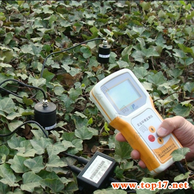
With the development of agriculture, the use of agricultural instruments such as soil moisture thermometers to assist in production during the production process is a more mainstream and more feasible approach, especially for the cultivation of characteristic fruits such as passion fruit and the use of soil moisture. The temperature meter measures the soil temperature, moisture content and changes in the process of crop growth and development, and is convenient for timely and appropriate irrigation, which has a very important role in improving the level of agricultural production and production quality.
Passion fruit is a fruit tree species in tropical and sub-tropical regions. It belongs to the perennial vine tree that is not tolerant to moisture and strong in drought resistance. Its optimum growth temperature is 20~30°C, and it grows well at temperatures not lower than 0°C. At -2°C, the plants will be seriously affected and even die. It can be seen that the growth of Passion fruit has certain requirements for temperature, moisture, light, and soil. However, manual cultivation is difficult to achieve fine management, and there is no way to truly meet the needs of crops. In the agricultural production, the use of soil moisture temperature instrument for scientific detection has been paid more and more attention. Through quantitative analysis and eliminating the influence of human error, it is also more conducive to carrying out activities in the correct mode of production to ensure the quality of passion fruit cultivation. To further expand production.
What is 4 layer PCB?
Compared with Double Sided PCB, multi-layer PCB have many advantages. They can be designed more compactly. They can greatly improve noise resistance and make layout easier.
4 layer PCB stackup and thickness


4-layer PCB has two stacking forms


For the following reasons, this may be a better stack to use a four-layer PCB:
When the high-speed signal changes the reference plane, there should be a nearby path for its return current to move between the two reference planes. Using two horizons, you can do this by connecting two planes directly to a single channel. For grounding and power layers, the connection must be made through capacitors, which usually require two through-holes and one capacitor. This means worse signal integrity and more circuit board occupancy. On the other hand, having a power plane can reduce the voltage drop on the power rail, thereby releasing the space on the signal layer.
PCB Board Thickness


4 layer PCB Prototype
4-layer circuit board prototyping refers to the trial production of printed circuit boards before mass production. It is mainly used for electronic engineers to design circuits and complete PCB Layout, then to carry out small-scale trial production process to the factory, that is, proofing PCB. The production quantity of four-ply proofing generally has no specific boundaries. Generally, engineers call it proofing before product design has not been confirmed and test has been completed.
Notices for proofing of four-layer circuit boards
The precautions for the production of four-layer PCB samples generally include two groups, one is the Engineer group, the other is the PCB sample manufacturer.
As a group of engineers, the matters needing attention in proofing are as follows:
1. Choose proofing quantity carefully to control cost effectively.
2. Specially confirm device packaging to avoid proofing failure due to packaging errors.
3. Conduct comprehensive electrical inspection to improve the electrical performance of PCB board.
4. Make good signal integrity layout, reduce noise and improve PCB stability.
As a manufacturer of four-layer circuit boards, the precautions are as follows:
1. Check PCB files carefully to avoid data problems.
2. Conduct process approval in an all-round way and process configuration with self-manufacturer.
3. Control production quantity, reduce cost and maintain quality.
4. Communicate with customers who need samples to prevent accidents in advance.
4 layer PCB price and cost
We specialize in Quick Turn PCB services with an industry leading turnaround time as fast as 24 hours. Three low-cost options for a small number of PCB prototyping needs. At the same time, we also provided Flexible PCB , Rigid-Flex PCB, Metal Core PCB, High-TG PCB, Aluminum PCB , PCB Stencils, PCB Assembly Services and so on. Using the same high-tech equipment as our full-service PCB, it can be manufactured quickly and with virtually no limits.
4 layer PCB manufacturing
We provide a full range of PCB functions to meet all your PCB needs. At present, we accept five PCB file formats (gerber file,.Pcb,.Pcbdoc.cam or.brd file format) for PCB manufacturing. But if you design a circuit board using Sprint-Layout software, you can send the. LAy6 file to us to manually generate the Gerber file.
JingHongyi PCB can provide you with multi-layer PCB board that meets RoHS standard. With laminated material, it can match high temperature in assembly process. It is important to remember that some lead-free assembly processes will require laminated substrates to withstand temperatures exceeding 260 degrees Celsius or 500 degrees Fahrenheit over a longer period of time. To solve this problem, we have high temperature laminates in stock, so that our customers can meet the higher temperature cycle requirements of some lead-free assembly applications.
Min. Order Quantity: 1 pcs
Material: FR-4
Finished Copper: 1oz/2oz/3oz(35μm/70μm/105μm)
Inner Layer Copper Thickness:1oz/1.5oz(35μm/50μm)
Silkscreen: White, Black, None
Surface Finishing: HASL with lead, HASL lead free, Immersion gold, Hard Gold ,OSP...
Shape: Custom Shape
100% Quality control
When making circuit boards, and after they are finished, we will test and inspect them strictly to ensure that the product reaches 100% eligibility rate. Preferential prices and higher quality have always been our constant pursuit:


Videos for 4 layer PCB design and manufacturing
Soil moisture temperature meter provides technical support for scientific planting of passion fruit